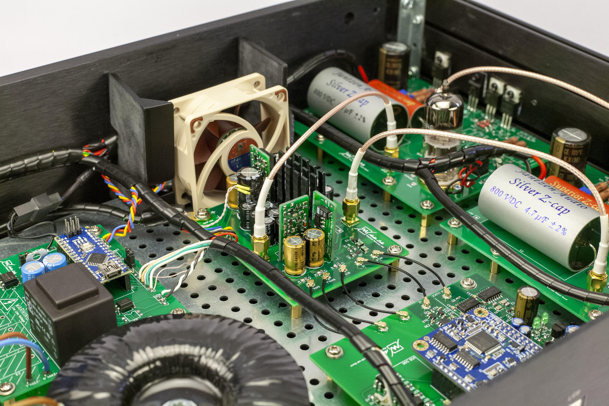
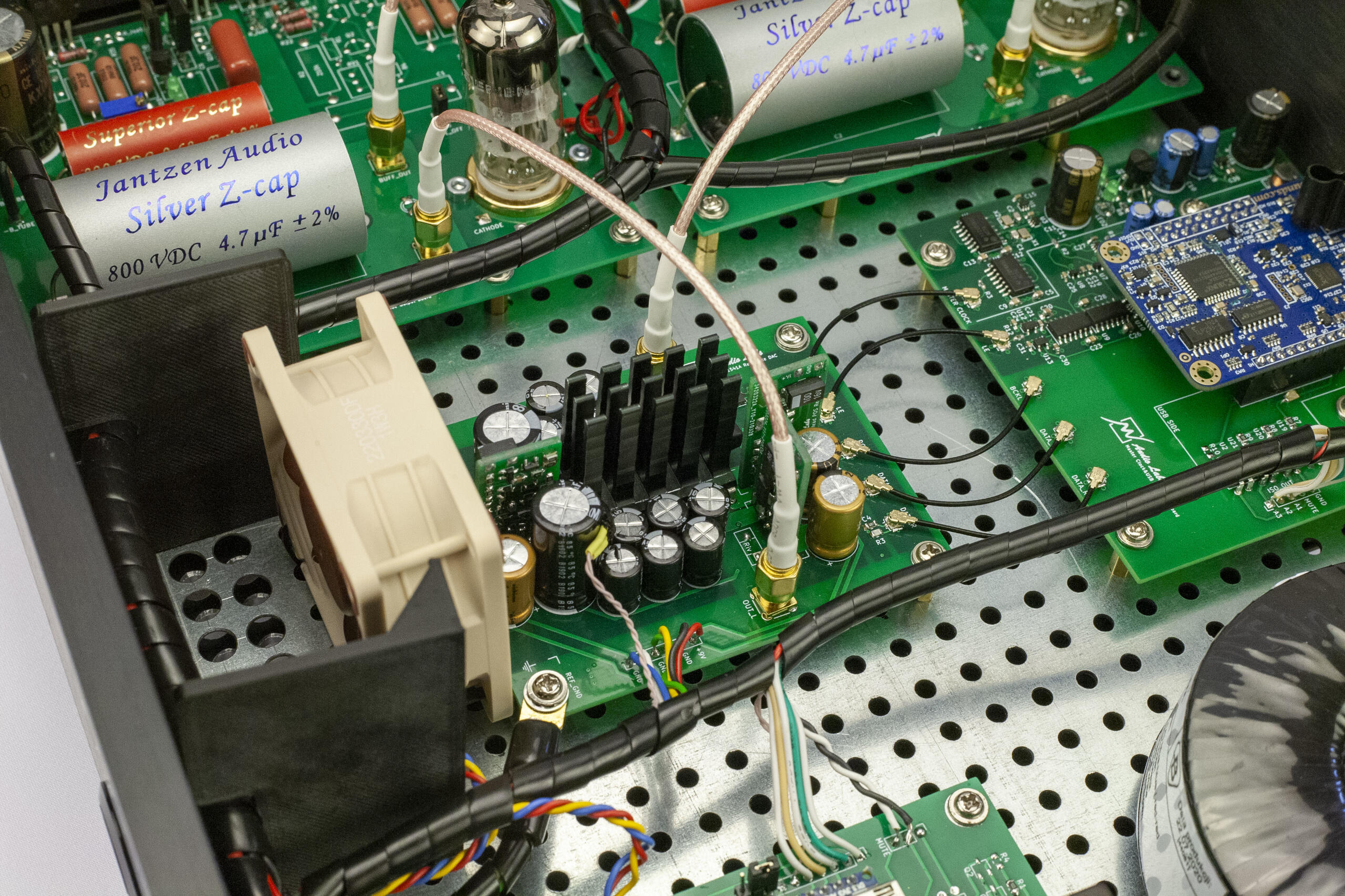
First of all the simultaneous data mode implementation is sub-optimal. It’s works and it’s correct as far as datasheet specs goes, but it’s very marginal. Sample conversion happens at LE signal positive edge, so we want to delay LE signal as much as possible after sample data stops. This way we initiate sample conversion during total digital silence (no ground bounce) and have the most accurate timing possible. But in scope-shot above we observe LE going positive together with bit-clock going negative. It works, as datasheet allows bit clock fall time to latch rise time of 0ns, but it mitigates the whole advantage of stopped bit-clock operation.
Next there was a firmware glitch that made my hair go grey for a long time. It manifested itself like a strange digital distortion when listening to a loud music passage. This obviously could be hundred different things so a digital interface wasn’t high on my list. Long story short, it’s a firmware bug that I was lucky enough to discover after 4 years of people buying and listening to this interface. Hurray!
It comes down to the way TDA1541 expects data to be in simultaneous mode. It should be in offset binary. When translated to human language this means that all digital zeros produce no current at output and all ones is full scale current. This is different than regular I2S data, where all digital zeros is half the output current. So to convert I2S data to simultaneous mode, one has to always invert the first bit. And here was the problem. When incoming data was all zeros, everything was converted fine. But when music contained negative clipping signal, which in I2S means first bit 1 and all others zeros, it wasn’t inverted by firmware and send straight to TDA “as-is” resulting in half signal current instead of zero (second pic above). The strangest part is that none of the usual wave signal generator software (SpectraPlus, ASIOTestSigGen, REW etc.) are outputting truly 0dBFS sine wave! They all must be doing some dithering or something. Hence there was no way to catch this bug when testing DAC with sine-waves. Something to watch out for I guess.