High-Voltage Lab Power Supply

Ok, first things first. I know the IEC definition of High Voltage. And yes – it’s above 1.5kV DC. But for me, high voltage is anything that can zap you for good. So let’s agree to disagree and call this 0.3kV PSU High Voltage, mmmkey?
So this was a long time coming. I had HV power supply on my “equipment to buy” list for, I don’t know… 10 years or so. It’s not often that I work with voltages higher then 60V or so, but when I do… It’s with tubes and I’m always frustrated because I have to mock up something quickly from some junk isolation transformer and hope that nothing gets shorted and melted (because of no current limiting).


My old HV rig for tube testing a.k.a “much safety”
Then I get angry and start browsing eBay for some surplus equipment, but everything is always “too heavy” to ship and/or “too roomy” for my bench space. After some time, frustration gets to a point where I start looking at new equipment offerings and then again – I’m astonished by the fact, that in this day and age, high voltage linear power supply’s are almost extinct. It’s considered a niche product and usually has to be made on order so prices can be astronomical. At this point a reality check is over and I get back to my daily routine.
And then, one fine day, I get a ring on my door and this package with a box from a good friend (thanks E.A.) arrives:


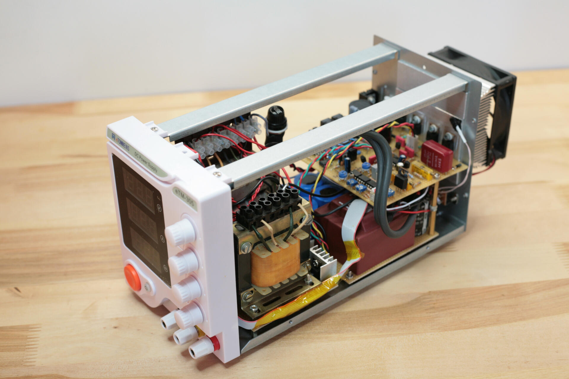
The case
I feel I have made enough cases for all kind of devices imaginable in my lifetime so this time decided to buy something instead. Of course your mileage may vary, so feel free to give it a go. Right stuff is usually not cheap, so be prepared to spend at least $50 for a general “project box” of adequate size. Or you can go for fancy aluminum one which will settle you $100 or more. Then there are knobs, switches, connectors, voltage and current display so at the end of the day you are looking at $100-$200 just for a box that looks like power supply. Not a good start by any means. So I started looking through Chinese markets for a dirt cheap “promo” power supply’s. And what do you know! They go as cheap as $50. Yes, shipping included.


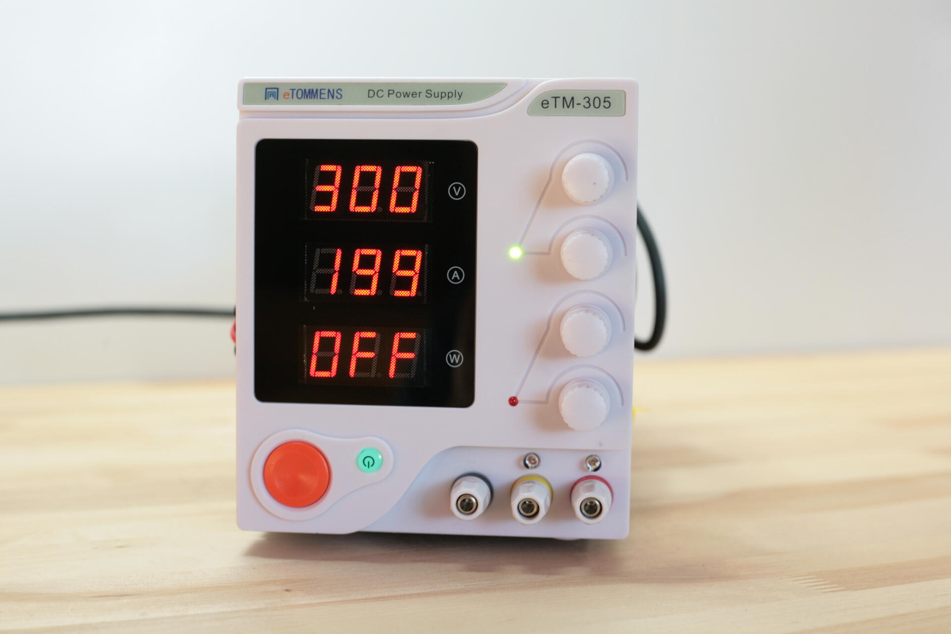
This one is called eTommens eTM-305 but I feel it’s some of their OEM design that you just stick your company name and list on Ali. And even when writing this I see it listed for $56 USD. That’s insane. And you know what the funny part is ? It actually works! I won’t do a review here, but my unit did met it’s specs and produced 20mVrms ripple @ 30V and 5A. That’s over 20Mhz BW which is impressive for a probably no more than $20USD locally priced product. I have no idea how they manage to do that, but then again – I’m no economist. Probably has something to do with mass-production and making ether from a thin air… What I do know is that now I have everything I need to proceed with my project.
Circuit design
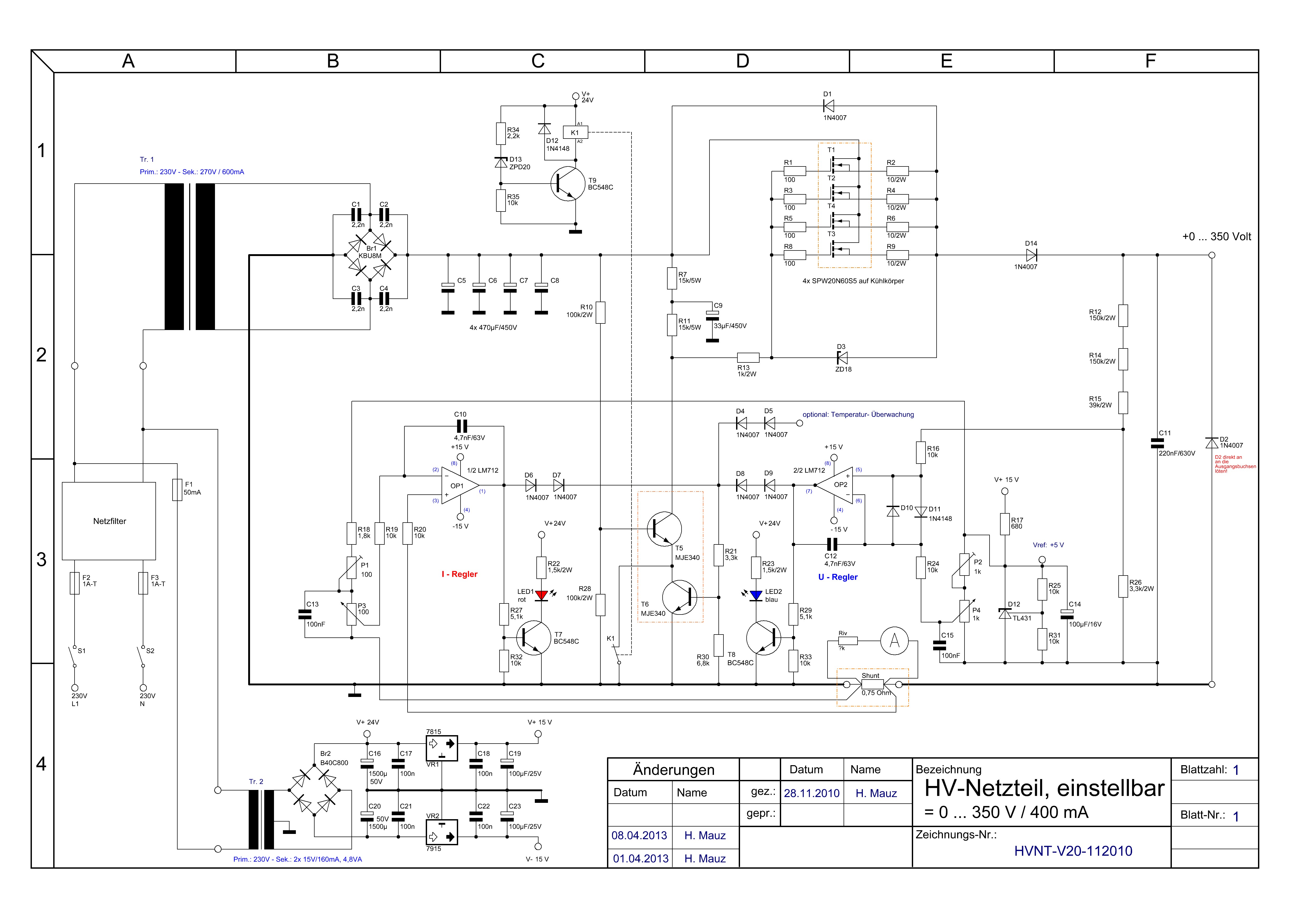
Or the lack of it I should say. I was planning this for so long that over the time I have accumulated a large amount of design ideas and I just couldn’t be bothered to do it from a scratch. So here it goes – this design is based on work by Horst Mauz and his “Labornetztei 350/400mA” schematics. Very minimalistic and basic design idea. One double op-amp and couple transistors – I like it. I mean, there isn’t a lot of ways to build a series voltage regulator and current limiter with op-amps. So I’m sure I would do it almost the same way even if I never saw it in the first place. But I digress.
Let’s get back to the basics. So how do you design a linear HV power supply ? Well, all the commercial designs that I saw (except really exotic ones) can be divided in two groups. Let’s call them “AC regulation” and “DC regulation”. Here is a couple of function block diagrams to better illustrate my point.

This is a “DC regulation” and is as basic as it gets. We have a positive ratio primary transformer connected to bridge rectifier feeding main reservoir cap. Then DC voltage is regulated by a transistor to a desired level and current sensing is used to limit it for a set value. Actually this is a block diagram of a circuit that I was referring to previously. This approach has one major problem though. In case of short circuit, our regulating transistor has to dissipate massive amount of heat. In our worst case scenario this would be 450V times 0.2A equal to 90W! (140W in original design, ouch…).

To battle this problem “AC regulation” is used. This has a few implementations but the main idea is to control AC voltage entering the main reservoir cap depending on a output voltage requirements.


This works reasonably well and with a modern SCR’s and careful layout can be really low noise. Although technically this IS a switching power supply, but we are switching mains voltage at a very low frequency. Only possible down side could be more involving SCR control circuitry, but nothing out of ordinary really.

And finally we arrive at the solution for improved “DC regulation”. Here we are switching our transformer secondaries depending on the DC voltage requirements. Very rudimentary solution. And very hard to screw it up. Efficiency is worse then with AC switching but hey! At least (almost) nothing is switching, right? So let’s go with it.
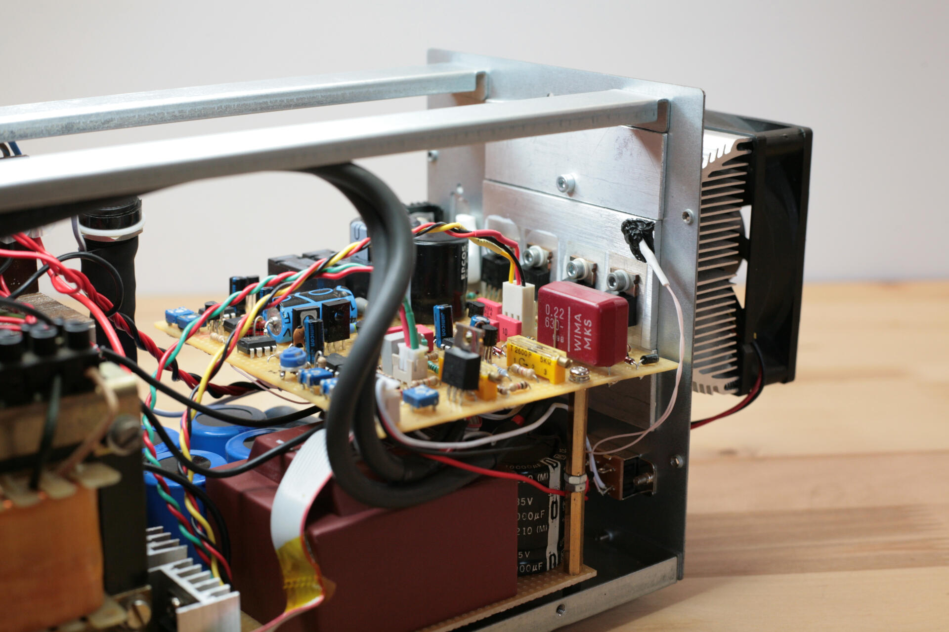
Schematics
Here is the final schematics “as build”. You can download a PDF for better viewing experience. Let’s go quickly trough it.


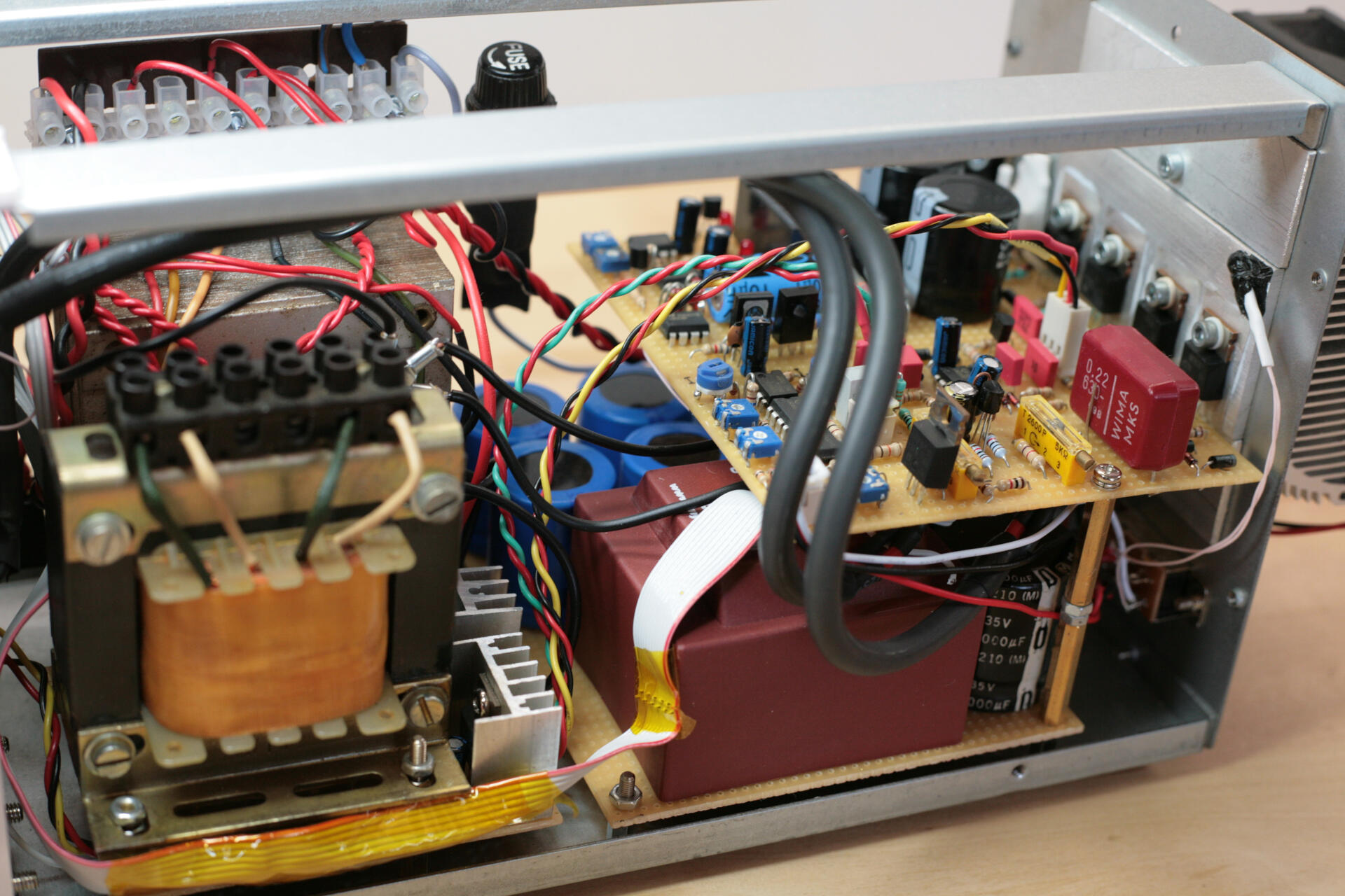
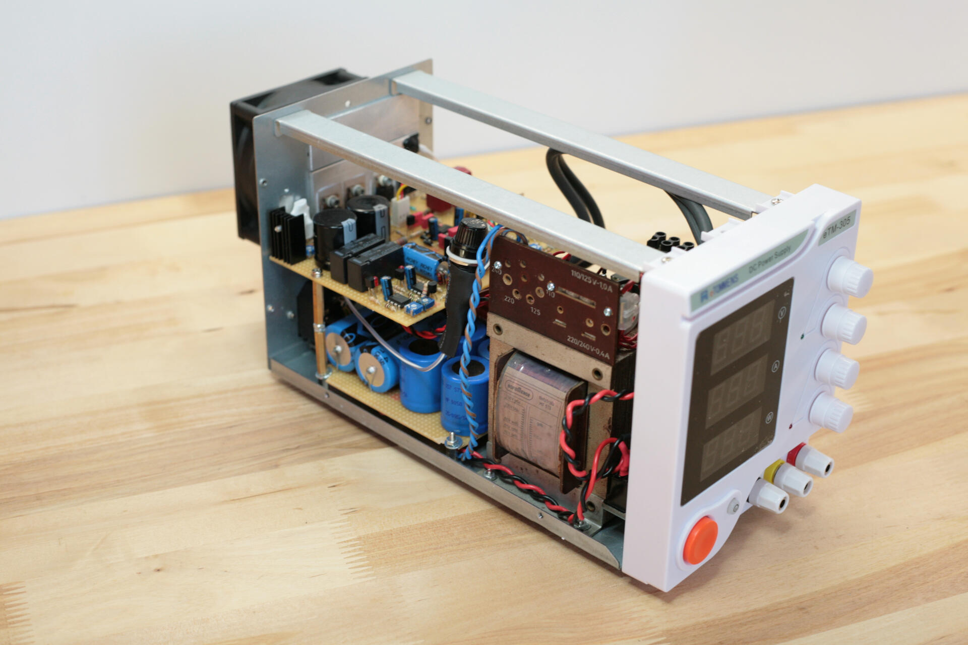
At the heart of this PSU is a transformer T1. It’s kinda tricky to find something like this now. Your best bet is online auctions and transformers from old Tektronix equipment. Luckily for me I had this old transformer from an ancient tube TV. It has a lot of primaries for different voltages (110V, 125V, 150V, 220V, 240V). So I just reverse connected secondary 230V winding to mains and now had a lot of secondaries. Unfortunately this wasn’t enough. At 200mA I had only 200V instead of 240V. Guess I was asking a little bit too much from these tiny secondary windings. So I had to use another old transformer in series and limit myself to only 300V DC after regulation. Not nice. But it’s not like I’m running out of that old iron any time soon.


Only new and in stock transformers that is usable here would be 230V Pri /2X115V Sec ones. For instance this TST 100/028 from INDEL would be good for 300V DC. And it should fit the case too. Of course you will be left with only two voltage taps, but it’s still twice less power dissipation.


I guess ±12V supply is self explanatory. T2 should be rated for at least 0.5A as in my case there was ~300mA current consumption on positive line. Next we have full wave bridge rectifier D5,D8,D9,D15 made of BYV26C. I especially encourage usage of “soft” or “fast” switching diodes in this position because of a non existing switching noise. Otherwise shunt diodes with some 1nF caps. C4 is a main reservoir cap and should be no less then 680uF and rated for 450V. More capacitance never hurts. 2.5A fuse is there in case stuff hits the fan. 680uF @450V is a LOT of energy and we are not welding anything here.
D6, D10 makes half wave rectifier for 300V BIAS output. R5 acts as fuse, Q1 is classics – ripple eater, virtual battery, active filter – so many names for such a simple thing. It just filters out AC and here it’s also zener D11, D13,D16 clamped to ~300V. Q2 should be on a small heat-sink as it acts as cascode for JFET Q3 current source and takes all the voltage drop in case of short-circuit. Q3 can be any N or P ch. JFET set to your desired current (just adjust its connection and source resistor accordingly).


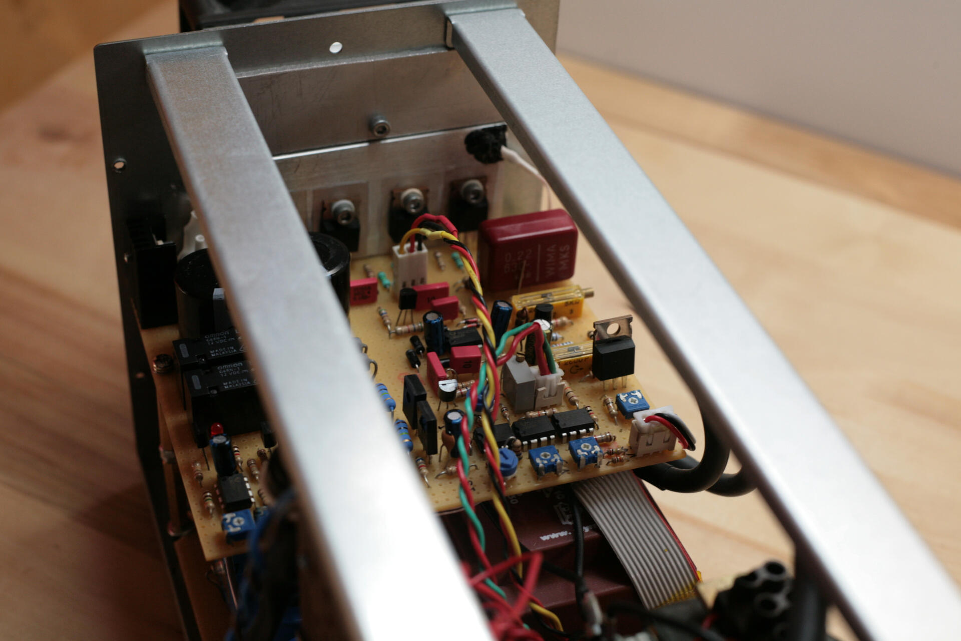
Here we have a main action. U3A acts as a current limiter. Positive OP-AMP input senses current trough R54 shunt resistor, compares it to a set voltage Ipot and pulls base of Q13 to open if there is over-current situation. Q13 pulls gates of regulating transistors Q5-Q8 to a ground thus setting output voltage to a level that results in a set current (CCS mode).
U3B acts as a voltage regulator, comparing output voltage from a 1:100 resistor divider R28, R57,58 to a set voltage Vset and opening base of Q13 to reach an equilibrium (CV mode). U4 generates reference voltage which is +5V. Q11 acts as a cascode and keeps Q13 collector at 1/2 supply voltage enabling usage of MJE340 past 300V and bringing all the benefits of a two stage cascode amplifier. R16, C7 compose an RC filter to help with PSRR and R22 acts as a current source. This trio could be replaced by a proper CCS, but with increased bandwidth comes more problems with stability. This could be attempted with a proper PCB but on a breadboard – really bad idea.
C8 acts as an output cap and should be no less than 220nF. C9, C10 BW limits current and voltage loops respectively. They can be altered slightly by looking at over-current shut-down and recovery overshoots on a scope. C11 compensation cap is needed to damp some HF ringing when current limiting kicks in. R39, R42 sets maximum current and voltage. Don’t mind 10kΩ and 1kΩ pots for current and voltage setting. That’s just what I had already on my units front panel. You can just use single 100Ω for current and 10kΩ for voltage.


Just remember that these are high impedance points and they are very susceptible to hum pickup. I had to use double-shielded balanced audio cable here. Cable routing should be careful too (don’t place it near transformers).
Everything else is for protection really. D28, D29 limits op-amp input diff. voltage to 0.7V, D24-D27 separates op-amp outputs, D20, D21 – protects mosfets gates, D19, D18 – prevents reverse biasing, D22, D23 – just in case output goes to >1kV and D19 fails.

Transformer secondaries switching is based on U1 and U2 that act as a comparators. 1MΩ feedback resistors adds a little bit of hysteresis to prevent relay shuddering. R2 and R10 sets first and second turn-over voltages. In normal CV mode, relays are switched depending on potentiometer voltage Vset. When overcurrent occurs, Q10 opens and disables Vset voltage. Now relays are operated depending on a real output voltage Vmeas. This is all needed primarily for a reliable start-up sequence. Q10, Q9, Q4 as well as Q12,Q14 can be any general small signal transistors (2N2222, BC550, BC547 etc.).


And finally we have some voltage buffering and subtraction done by U5 and U6. There is about 10mA of standing current through resistor R54, so U5B and U6B takes care of that permanent voltage drop.
Q15 makes a very basic temperature fan control. Place R55 on a main heat-sink and adjust R61 to turn FAN on when desired temperature is reached.
Interfacing to a display
This wasn’t very straight forward and looking back I probably should’ve ditched the display board and went for some general LED voltmeter kit.


But I didn’t. So if anyone else wants to be as stubborn as me, here is how you do it (you’ve been warned though).


On my unit, data to a display driver is supplied by an Nuvoton 1T 8051-based Microcontroller N76E003. Pins 1,2 and 19, 20 are configured as analog inputs and they are sampling voltage for appropriate display. So far so good. What is strange and doesn’t make any sense is why they introduced a voltage offset when calculating display values. So for voltage – offset is 55mV to display 1V and for current – offset is 0.4V! to display 1mA. What a nonsense.
I didn’t reverse engendered whole unit just to find out what exactly BS reason they have to do this, but yeah… even in 2020 Chinese engineering marvels are not disappointing. After the offset, scaling is 8.5mV/1mA and 13mV/1V for set voltage and 0.75mV/1V for measured voltage. Again – What? Why? Whatever… So there is some (a lot actually) arithmetic’s to be done.


First we generate appropriate offset with R99,R71 and R76. Then we add it to a respective voltages using U7A,U8A and amplify it with U7B,U8B. Vmeas has to be scaled down by R75,R77 before amplification.


Same thing with currents, just Imeas doesn’t need scaling. I made all gain stages adjustable so it would be easy to deal out exact values needed. But story doesn’t end here. Dots on displays were all at the wrong places.


So I just cut off the tracks to pin number 3 on all displays and wired them manually. Maybe there was a more elegant solution, but at that time my patience was running really low.


Voltage display has to show second dot when setting the voltage below 100V. This is achieved with U11A. But wait! All three dots are illuminated! Yes, they are. But that’s what black insulating tape was invented for 🙂 So just stick it were needed and be done. Same story with power display dot. It should be illuminated only when output is on. This is ensured by Q19 and Q20. Source of base voltage for Q19 is pin16 of MCU which is HIGH when output is ON. Q20 collector is also controlling output relay that is connected to negative supply (as well as fan) to lower the load on positive 12V rail.
The result
Here are some scope shots I took while tinkering with this frankenstein.

This is a worst case scenario step response. 300V open line to a 200mA limited short circuit and back to open line. On the left you can see zoomed in short circuit moment. Overall not a bad result for a breadboard design.

And here is output noise. Around 5mVpp at open line and 20mVpp at 200mA load current (@300V). Also very reasonable all considered.